Services and Engineering: IV
Antisticking-coating service:
Antisticking layers (ASL) are available for replication tools as well as for lithography-masks.
ASL are a very useful added functionality to our products when easy mold-separation is essential for your replication process.
We do also offer anti-sticking coatings for lithography-masks. An additional ASL can become the best measure to reduced sticking forces between mask and resist-coating. This is very helpful way to avoid mask-contamination due to resist-voids, thus increasing "operating-hours-between-cleaning". This is particularly crucial with thick resists (e.g SU-8) and -inherently- long exposure durations.
Our ASL coatings still allow the use of organic solvents (Aceton, IPA, etc.) for intermediate mask-cleaning.
Antisticking-coatings are Si-F based and can be refreshed and thereby substantially extending mask-life.
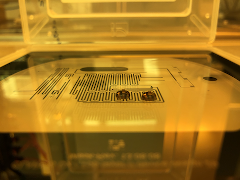
1: Antisticking layer (ASL) on 5inch Mask to avoid defects during hard-contact exposure.
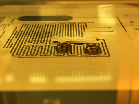
2: Antisticking layer (ASL) on 5inch Mask to avoid defects during hard-contact exposure.
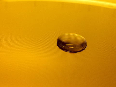
3: Antisticking layer (ASL) on Nickel-mold for PDMS casting.
4: Antisticking layer (ASL) on Nickel-mold for PDMS casting.
5: Antisticking layer (ASL) on Nickel hot-embossing stamp.
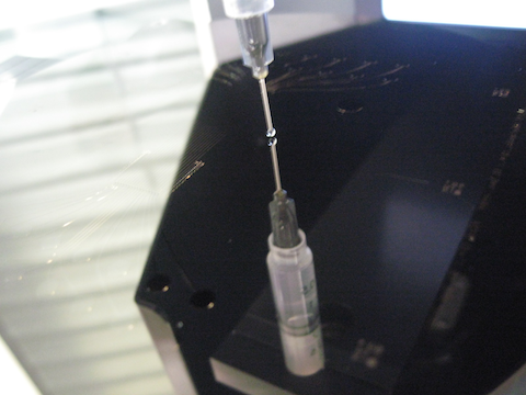
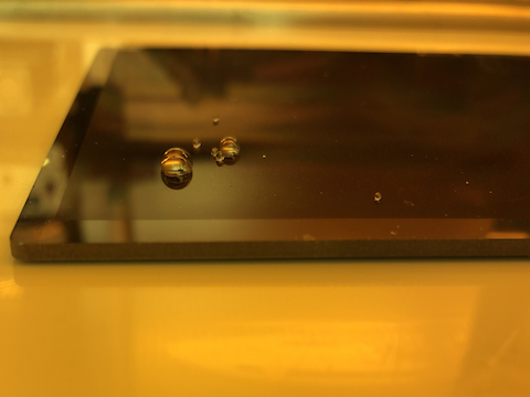
6: Wetting-angle measuring procedure.
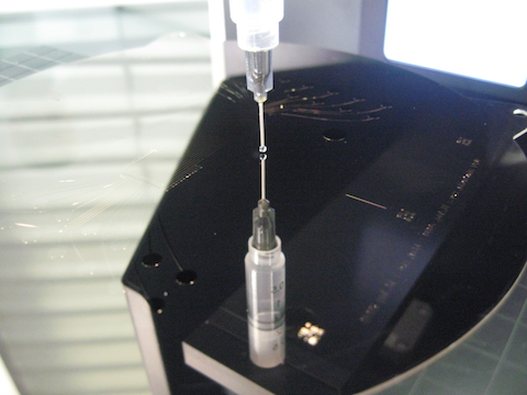
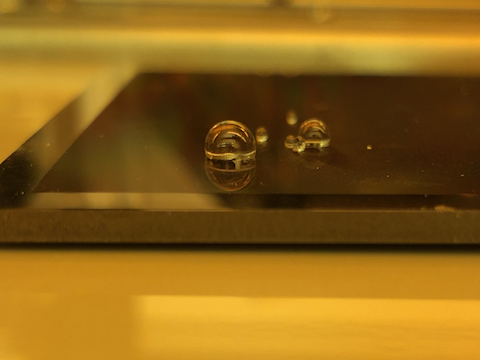
7: Wetting-angle measuring procedure.
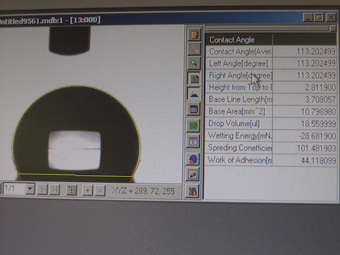
8: Measuring protocol: wetting-angle = 113.2°
Specifications:
Type of the ASL-coating:
Fluoro-Silane.
Additional SiO2 base coating may be required (Thickness = 20 - 50nm)
Coating available for these substrate materials:
Glass (e.g.Sodalime or Quarz for lithography-masks)
Silicon, Nickel, Steel
Substrate formats:
Round substrates: ø100 - ø300mm
Square substrates: 4", 5", 6", 7", 9"
Replication tools: any shape of shims, stamps or inserts
Process flexibility:
Other substrate-formats or substrate-material on request.
1. Customer sends pattern-design (CAD-file, sketch,...)
2. applied microSWISS takes care of maskset-manufacturing
3. SiO2 coating (thickness = 50nm) onto mask
4. CVD processing to apply Antisticking coating
5. Packaging processed mask in original container
6. Shipping with appropriate remarks for handling, cleaning and storage
1. Customer sends pattern-design (CAD-file, sketch,...) for stamp
2. applied microSWISS to manufactures the hot-embossing stamp
3. SiO2 coating (thickness = 50nm) onto mask
4. CVD processing to apply Antisticking coating
5. Packaging processed stamp in appropriate container
6. Shipping with appropriate remarks for handling, cleaning and storage